This fab will be constructed with an investment of Rs 91,000 crore, said Union IT Minister Ashwini Vaishnaw….reports Asian Lite News
The Union Cabinet, chaired by Prime Minister Narendra Modi, on Thursday approved the establishment of three semiconductor fabrication (fab) units that will start construction within the next 100 days and generate direct employment of 20,000 advanced technology jobs and nearly 60,000 indirect jobs.
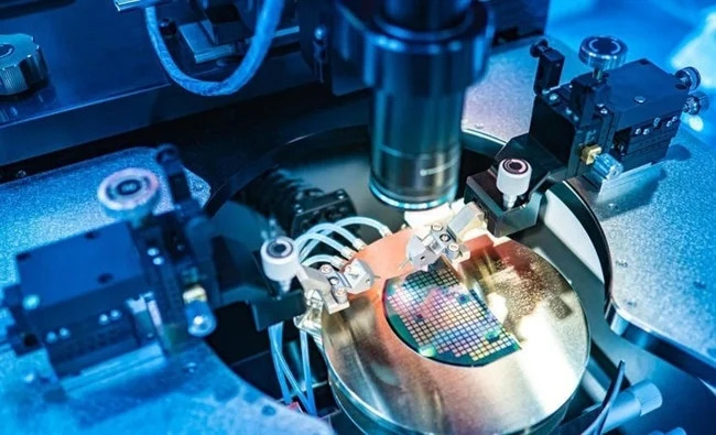
The semiconductor fab with 50,000 wafers per month capacity will be set up by Tata Electronics Private Ltd (TEPL) in partnership with Powerchip Semiconductor Manufacturing Corp (PSMC), Taiwan, in Dholera, Gujarat.
This fab will be constructed with an investment of Rs 91,000 crore, said Union IT Minister Ashwini Vaishnaw.
This fab will cover high-performance compute chips with 28 nm technology, and power management chips for electric vehicles (EVs), telecom, defence, automotive, consumer electronics, display, power electronics, etc, according to the government.
Another semiconductor assembly, testing, monitoring, and packing (ATMP) unit with a capacity of 48 million per day by Tata Semiconductor Assembly and Test Pvt Ltd (TSAT) in Morigaon, Assam, will be set up with an investment of Rs 27,000 crore.
TSAT semiconductor is developing indigenous advanced semiconductor packaging technologies including flip chip and ISIP (integrated system in package) technologies. It will cover sectors like automotive, electric vehicles, consumer electronics, telecom and mobile phones, etc, according to the government.
The third semiconductor ATMP unit for specialised chips will be set up by CG Power, in partnership with Renesas Electronics Corporation, Japan and Stars Microelectronics, Thailand in Sanand, Gujarat.
“This unit with a capacity of 15 million per day will be set up with an investment of Rs 7,600 crore,” the Centre said.
The CG power semiconductor unit will manufacture chips for consumer, industrial, automotive, and power applications.
Within a very short time, the India Semiconductor Mission has achieved four big successes. With these units, the semiconductor ecosystem will get established in India.
India already has deep capabilities in chip design. With these units, the country will develop capabilities in chip fabrication. Advanced packaging technologies will be indigenously developed in India with Thursday’s announcement. These units will accelerate employment creation in downstream automotive, electronics manufacturing, telecom manufacturing, industrial manufacturing, and other semiconductor consuming industries.
The ‘Programme for Development of Semiconductors and Display Manufacturing Ecosystem’ in India was notified in 2021 with a total outlay of Rs 76,000 crore. In June last year, the Cabinet had approved the proposal of US-based Micron for setting up a semiconductor unit in Sanand, Gujarat. Construction of this unit is progressing at a rapid pace and a robust semiconductor ecosystem is emerging near the unit.
Samsung Opens New R&D Facility
Samsung Semiconductor India Research (SSIR) on Thursday announced the opening of its new research and development (R&D) facility in the country.
This is SSIR’s second office in Bengaluru, with a capacity to accommodate close to 1,600 professionals.
Located at Bagmane Capital Tech Park in Angkor-West area, the facility spans 1,60,000 square feet across four floors, the company said in a statement.
“The new facility embodies our commitment to expanding our footprint in India,” said Balajee Sowrirajan, EVP and MD at SSIR.
SSIR currently has a strength of over 4,500 employees and will add over 700 people, including fresh graduates as well as lateral hires across teams in the country.
SSIR recently collaborated with the Indian Institute of Science (IISc) to help set up a Quantum Technology Lab.
The Quantum Technology Lab will integrate cryogenic control chip with qubits, single photon sources, and detectors, and address reliability challenges in quantum technologies.
The lab will serve as a centre for technological innovation, manpower training, and collaboration with national and international quantum research institutions, according to the company.
ALSO READ: Retail Market Eyes $2 Trillion by 2030

